Diplomarbeit
Platinenlayout (Speicherkarte)


Die folgenden Abbildungen zeigen die vom EAGLE-Programm XPLOT erzeugte Gerber-Photoplotterdateien für die Herstellung der verschiedenen Lagen der Platine, sowie die Excellon-Bohrdatei für die Platzierung der Bohrungen auf der Platine.
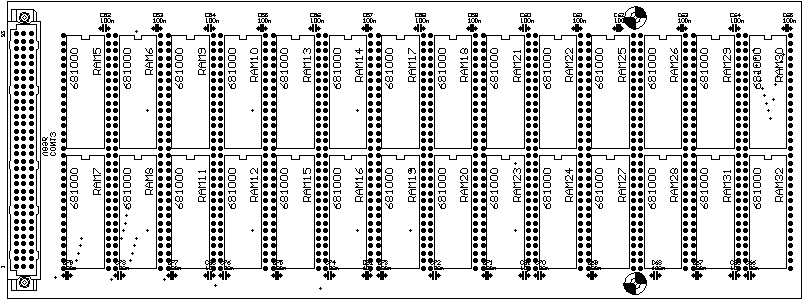
Bild 67: Platinenlayout des BISU-P-SPEICHERS Baugruppen
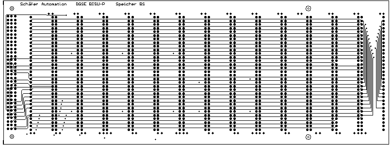
Bild 68: Platinenlayout des BISU-P-SPEICHERS Bauteilseite
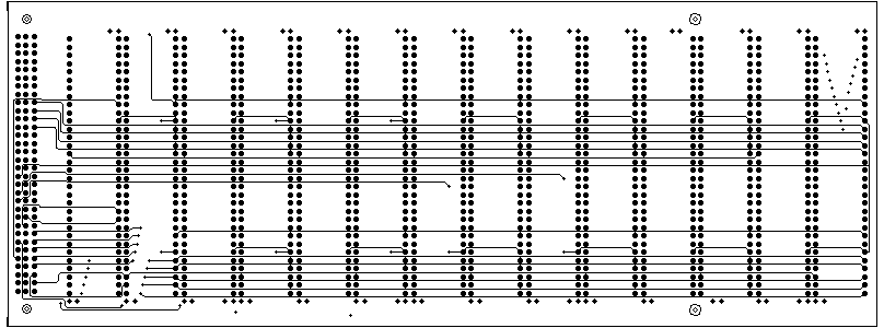
Bild 69: Platinenlayout des BISU-P-SPEICHERS Signallage 2
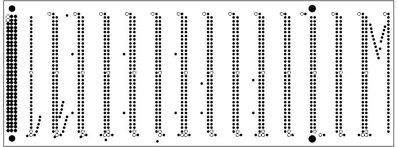
Bild 70: Platinenlayout des BISU-P-SPEICHERS Versorgungslage GND (Vollschicht)
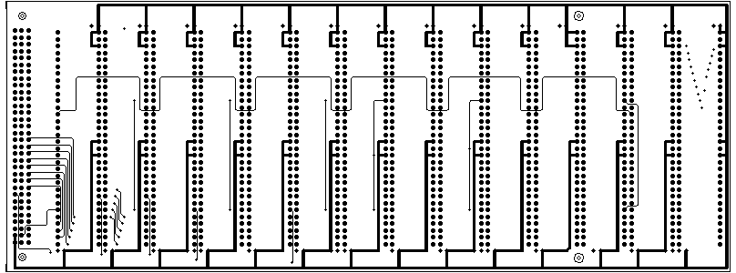
Bild 71: Platinenlayout des BISU-P-SPEICHERS Signallage 3
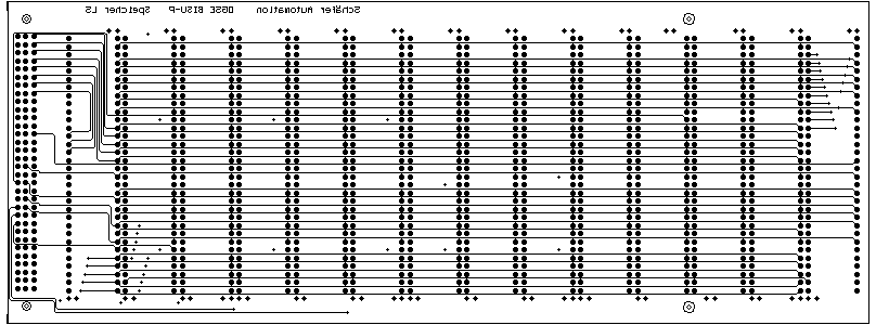
Bild 72: Platinenlayout des BISU-P-SPEICHERS Lötseite
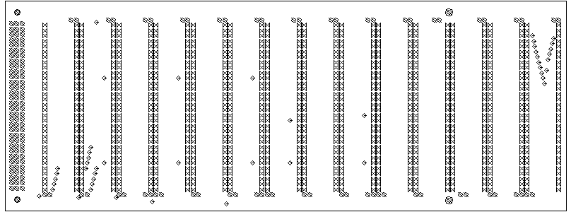
Bild 73: Platinenlayout des BISU-P-SPEICHERS Bohrungen
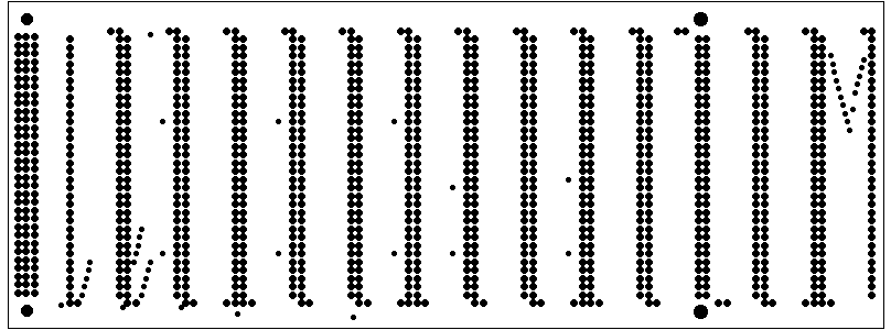
Bild 74: Platinenlayout des BISU-P-SPEICHERS Lötstoppmaske (Bauteilseite)

Bild 75: Platinenlayout des BISU-P-SPEICHERS Lötstoppmaske (Lötseite)